 |


The heterostructure laser. The integrated circuit — the chip
|
|
|
|
The heterostructure laser
Heterostructures have been crucially important for the development of semiconductor lasers. Zhores I. Alferov of the Ioffe Institute of the Russian Academy of Sciences in what was then Leningrad and Herbert Kroemer then at Varian in Palo Alto proposed in 1963, independently of each other, the principle for the heterostructure laser, an invention that is probably as significant as that of the heterotransistor.
Alferov was the first to succeed in producing a lattice-adapted heterostructure (AlGaAs/GaAs, 1969) with clear borders between the layers. Alferov's research team succeeded in rapidly developing many types of components built up of heterostructures, including the injection laser which Alferov patented in 1963. A technological breakthrough occurred around 1970 when heterostructure lasers became able to work continuously at room temperatures. These properties have, for example, made fibre-optic communications practically possible.
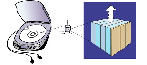 Fig. 2. The laser diode of the CD player contains a semiconductor heterostructure.
|
The integrated circuit — the chip
The invention of the transistor just before Christmas 1947 is usually taken to mark the start of the development of modern semiconductor technology (Nobel Prize in Physics 1956 to William B. Shockley, John Bardeen and Walter H. Brattain). With the transistor there came a component that was considerably smaller, more reliable and less energy-consuming than the radio valve, which thus lost its importance. The increasing complexity of a system using more and more radio valves meant that a practical limit had been reached with around a thousand valves. By soldering individual transistors together on a printed-circuit board the system could be increased to over ten thousand transistors.
Even though the transistor permitted an increase in the complexity of a system of individual components soldered together it soon became clear that the number of transistors was the limiting factor in meeting the needs of the emerging computer industry. As early as the beginning of the 1950s there were ideas and thoughts about manufacturing transistors, resistors and condensers in a composite semiconductor block, an integrated circuit.

|
| Fig 3. Development has gone from radio valves via transistors to integrated circuits, chips, now in all modern electronics |
The people who were to demonstrate the practical possibility of an integrated circuit were two young engineers, Jack S. Kilby and Robert Noyce, working independently of each other. Kilby, however, was first with his patent application and Noyce knew of this work when he filed his own application.
The integrated circuit is more of a technical invention than a discovery in physics. However it is evident that it embraces many physical issues. One example is the question of how aluminium and gold, which are part of an integrated circuit, differ regarding their adhesion to silicon. Another question is how to produce dense layers that are only a few atoms thick.
|
|
|
It is thus obvious that the development of the integrated circuit prompted enormous investment in research and development in solid-state physics. This has not only led to development in semiconductor technology but also to gigantic development of apparatus and instruments. Continual miniaturisation, moreover, has come up against a number of material-physical limitations and problems that have had to be solved.
The notion of an integrated circuit was there. But ten years were to pass from the invention of the transistor before the technology involved had matured sufficiently to allow the various elements to be fabricated in one and the same basic material and in one piece. The invention is one in a series of many that have made possible the great development of information technology. The integrated circuit is still, after 40 years, in a dynamic phase of development with no sign of flagging.
Jack S. Kilby and Robert Noyce are both considered as the inventors of the integrated circuit. Kilby was the one who built the first circuit. Noyce developed the circuit as it was later to be manufactured in practice with silicon and silicon dioxide as semiconductor and insulator and with aluminium as the electrically conductive element. Both have on a number of occasions received prizes and distinctions.
Robert Noyce died in 1990. He was then honoured as one of the most important founders of Silicon Valley and for the leading role his company had played in the development of information technology, with the integrated circuit as a cornerstone.
Jack S. Kilby has continued his career as an inventor, with some 60 patents. Among other things, he is co-inventor of the pocket calculator, one of the first applications of the integrated circuit. A market survey run before the start of planning for its manufacture showed that interest in a pocket calculator was negligible. After all, people had slide-rules!
(http: //www. nobelprize. org/nobel_prizes/physics/laureates/2000/public. html)
|
|
|